


 |
ECE602S - ELECTRICAL CIRCUIT AND ELECTRONIC - 1ST OPP - NOVEMBER 2024 |
|
|
1 Page 1 |
▲back to top |
nAml BIA UnlVERSITY
OF SCIEnCE AnDTECHnDLOGY
FacultyofHealthN, atural
ResourceasndApplied
Sciences
Schoolof Natural and Applied
Sciences
Department of Biology,
Chemistryand Physics
13Jackson Kaujeua Street
Private Bag 13388
Windhoek
NAMIBIA
T: +264 612072012
F: +264 61207 9012
E: dbcp@nust.na
W: www.nust.na
QUALIFICATION : BACHELOR OF SCIENCE
QUALIFICATION CODE: 07BOSC
COURSE:ELECTRICALCIRCUIT AND ELECTRONIC
DATE: NOVEMBER 2024
DURATION: 3 HOURS
LEVEL:6
COURSECODE: ECE602S
SESSION: 1
MARKS: 100
FIRST OPPORTUNITY: EXAMINATION PAPER
EXAMINER:
MODERATOR:
INSTRUCTIONS
MR. MARKUS HITILA
DR. VAINO INDONGO
1. Answer all questions on the separate answer sheet.
2. Please write neatly and legibly.
3. Do not use the left side margin of the exam paper. This must be allowed for the
examiner.
4. No books, notes and other additional aids are allowed.
5. Mark all answers clearly with their respective question numbers.
PERMISSIBLE MATERIALS:
1. Scientific Calculator
This paper consists of five pages including this front page
|
|
2 Page 2 |
▲back to top |
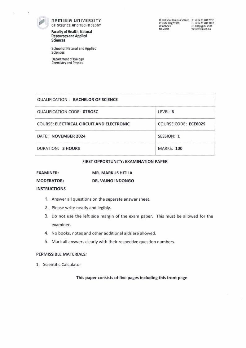
Question 1
(10)
The current through and voltage across an element is shown in Figure 1. Find the resulting
power and sketch the power delivered to the element fort> 0.
i(t) _ { 2t O < t < 15s
- -3t + 75 15s < t < 25s
30V O < t < 10s
v(t) = ( -St+ 80 10s < t < 15s
SV 15s < t < 25s
__ ,_ + V
i (A) ;.
30 ........................ .
V (V) A
30 i-i --~
5
5 10 15 20 25
t (s)
5 10 15 20 25
t (s)
Figure 1: Characteristic of current and voltage of the element
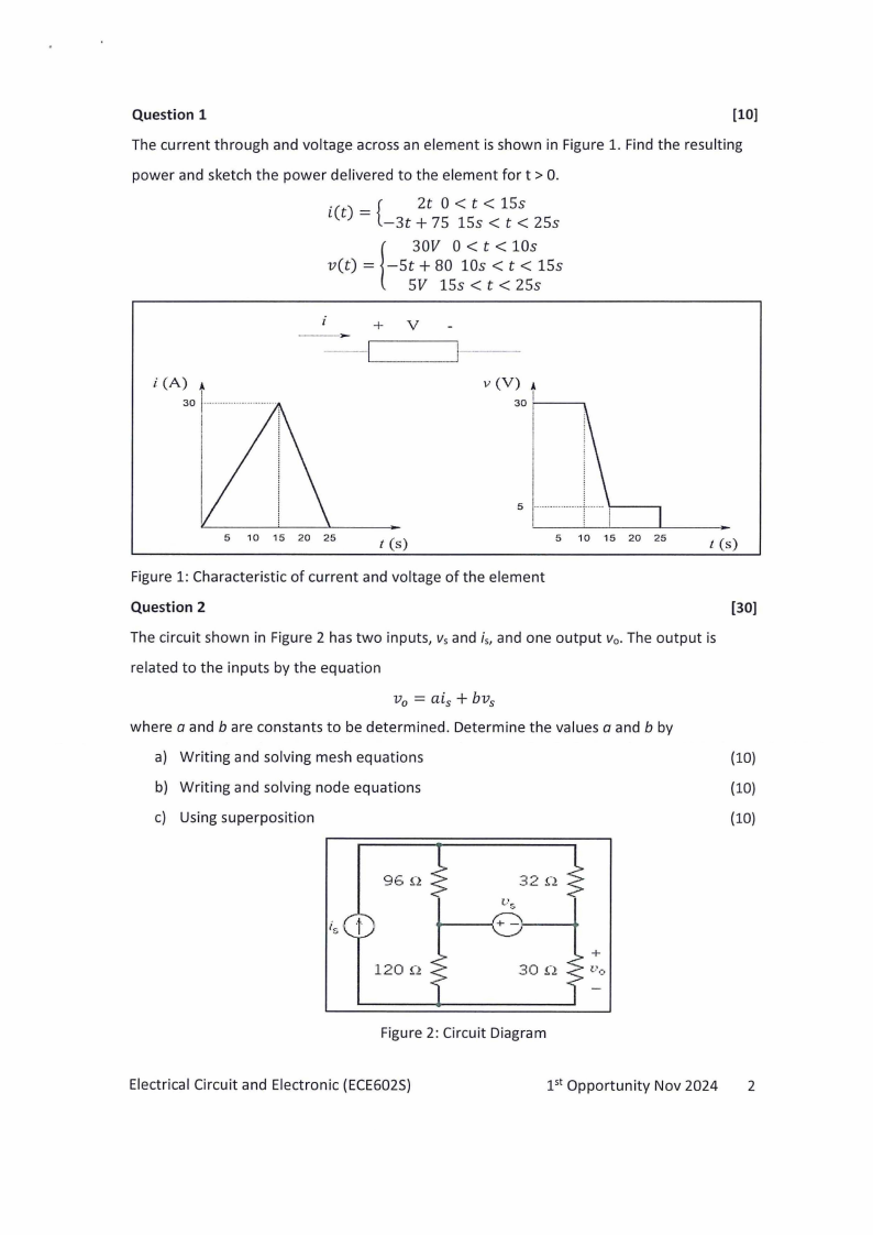
Question 2
[30)
The circuit shown in Figure 2 has two inputs, Vs and is, and one output v0 • The output is
related to the inputs by the equation
= V0 ai 5 + bv5
where a and bare constants to be determined. Determine the values a and b by
a) Writing and solving mesh equations
(10)
b) Writing and solving node equations
(10)
c) Using superposition
(10)
orI::, !J:
i$ t
120 f.!
32 !.::1:
Us
+-
+
30 £");
v.V
Figure 2: Circuit Diagram
Electrical Circuit and Electronic (ECE602S)
pt Opportunity Nov 2024 2
|
|
3 Page 3 |
▲back to top |
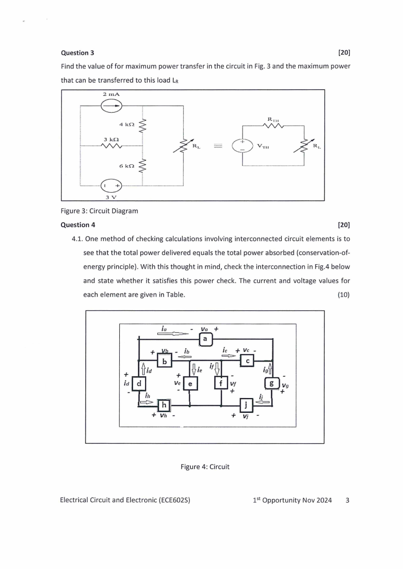
Question 3
[20)
Find the value of for maximum power transfer in the circuit in Fig. 3 and the maximum power
that can be transferred to this load LR
2 ruA
41<0
3 kn.
6k0
3V
Figure 3: Circuit Diagram
Question 4
[20)
4.1. One method of checking calculations involving interconnected circuit elements is to
see that the total power delivered equals the total power absorbed (conservation-of-
energy principle). With this thought in mind, check the interconnection in Fig.4 below
and state whether it satisfies this power check. The current and voltage values for
each element are given in Table.
(10)
------=-:i:a-::a:::::=- - Va +
+
--=ib
ic
+ Vh -
~+Vg
+ Vj -
Figure 4: Circuit
Electrical Circuit and Electronic (ECE602S)
pt Opportunity Nov 2024 3
|
|
4 Page 4 |
▲back to top |
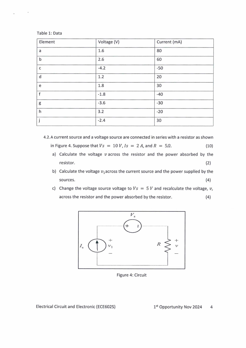
Table 1: Data
Element
a
b
C
d
e
f
g
h
j
Voltage (V)
1.6
2.6
-4.2
1.2
1.8
-1.8
-3.6
3.2
-2.4
Current (mA)
80
60
-50
20
30
-40
-30
-20
30
4.2. A current source and a voltage source are connected in series with a resistor as shown
in Figure 4. Suppose that Vs = 10 V, ls = 2 A, and R = Sfl.
(10)
a) Calculate the voltage v across the resistor and the power absorbed by the
resistor.
(2)
b) Calculate the voltage v1 across the current source and the power supplied by the
sources.
(4)
= c) Change the voltage source voltage to Vs 5 V and recalculate the voltage, v,
across the resistor and the power absorbed by the resistor.
(4)
+
+
V1
R
V
Figure 4: Circuit
Electrical Circuit and Electronic (ECE602S)
l51 Opportunity Nov 2024 4
|
|
5 Page 5 |
▲back to top |
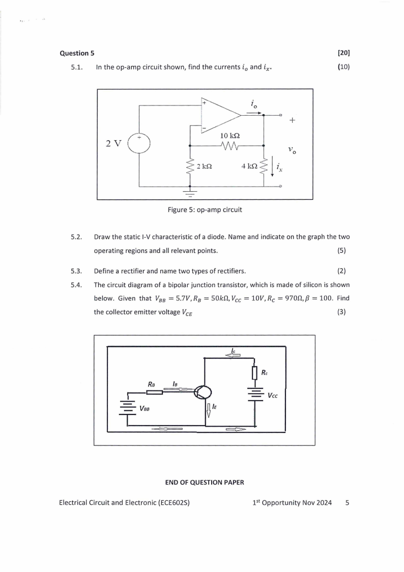
Question 5
[20)
5.1. In the op-amp circuit shown, find the currents i0 and ix·
(10)
-----------<
+
+
< 2 k.Q
. :OkQ
'\\./\\;/\\~--
V
j0
4 kQ :?. i .
~-:-:.;.> ,;\\.
Figure 5: op-amp circuit
5.2. Draw the static 1-Vcharacteristic of a diode. Name and indicate on the graph the two
operating regions and all relevant points.
(5)
5.3. Define a rectifier and name two types of rectifiers.
(2)
5.4. The circuit diagram of a bipolar junction transistor, which is made of silicon is shown
below. Given that V88 = 5.7V, R8 = SOkD.,Vee = lOV, Re = 970D.,/3= 100. Find
the collector emitter voltage Vee
(3)
r-
-=-vaa
L
<=le
Re
-=-vcc
OIE
==::::=-
END OF QUESTION PAPER
Electrical Circuit and Electronic (ECE602S)
l51 Opportunity Nov 2024 5