


 |
ECE602S - ELECTRICAL CIRCUIT AND ELECTRONICS - 1ST OPP - NOV 2022 |
|
|
1 Page 1 |
▲back to top |
nAmlBIA unlVERSITY
OF SCIEnCE Ano TECHnOLOGY
FACULTYOF HEALTH,NATURALRESOURCESAND APPLIEDSCIENCES
DEPARTMENTOF NATURALAND APPLIEDSCIENCES
QUALIFICATION: BACHELOR OF SCIENCE (MAJOR AND MINOR}
QUALIFICATION CODE:07BOSC
LEVEL:6
COURSENAME: ELECTRICALCIRCUIT AND
ELECTRONICS
COURSECODE: ECE602S
SESSION:NOVEMBER 2022
DURATION: 3 HOURS
PAPER:THEORY
MARKS: 100
EXAMINER (S)
MODERATOR:
FIRSTOPPORTUNITYEXAMINATION QUESTION PAPER
MR EMMANUEL EJEMBI
PROF. SYLVANUS ONJEFU
INSTRUCTIONS
1. Write all your answers in the answer booklet provided.
2. Read the whole question before answering.
3. Begin each question on a new page.
PERMISSIBLEMATERIALS
Scientific Calculator
THIS QUESTIONSPAPERCONSISTSOF 9 PAGES{Including this front page)
1
|
|
2 Page 2 |
▲back to top |
1.7 Which one of the following rectifiers was made with only one diode?
(2)
a. Full wave
b. Half wave
c. Both a and b
d. None of the above
1.8 Which one of the following has two or more junction devices?
(2)
a. Thyristor b. Transistor c. Diodes d. None of these
1.9 A transistor is said to be in quiescent state when
(2)
a. It is unbiased
b. No Current flows through it
c. Emitter junction is just biased equal to collector junction.
d. No signal is applied to the input
1.10 In a pnp transistor, the current carriers are
(2)
a Acceptor ions b. Donor ions c. Free electrons d. Holes
1.11 Most of the majority carriers from the emitter
(2)
a. Recombine in the base
b. Recombine in the emitter
c. Passthrough the base region to the collector
d. None of these.
3
|
|
3 Page 3 |
▲back to top |
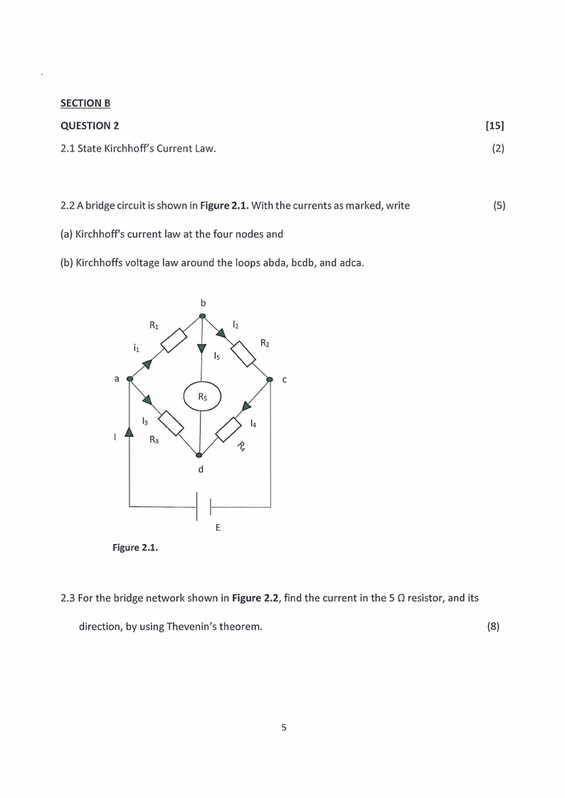
SECTION B
QUESTION 2
2.1 State Kirchhoff's Current Law.
2.2 A bridge circuit is shown in Figure 2.1. With the currents as marked, write
(a) Kirchhoff's current law at the four nodes and
(b) Kirchhoffs voltage law around the loops abda, bcdb, and adca.
b
a
C
[15]
(2)
(5)
d
E
Figure 2.1.
2.3 For the bridge network shown in Figure 2.2, find the current in the 5 0 resistor, and its
direction, by using Thevenin's theorem.
(8)
5
|
|
4 Page 4 |
▲back to top |
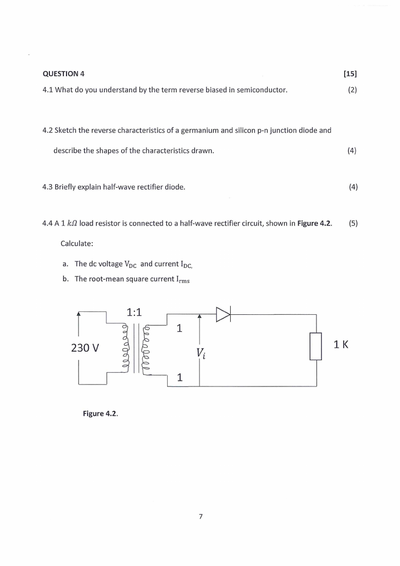
QUESTION 4
4.1 What do you understand by the term reverse biased in semiconductor.
[15]
{2}
4.2 Sketch the reverse characteristics of a germanium and silicon p-n junction diode and
describe the shapes of the characteristics drawn.
(4)
4.3 Briefly explain half-wave rectifier diode.
(4)
4.4 A 1 kfl load resistor is connected to a half-wave rectifier circuit, shown in Figure 4.2.
(5)
Calculate:
a. The de voltage Voe and current 10 c,
b. The root-mean square current Irms
1:1
1
LJ.- 230V
Vl,-
1
1K
Figure 4.2.
7
|
|
5 Page 5 |
▲back to top |
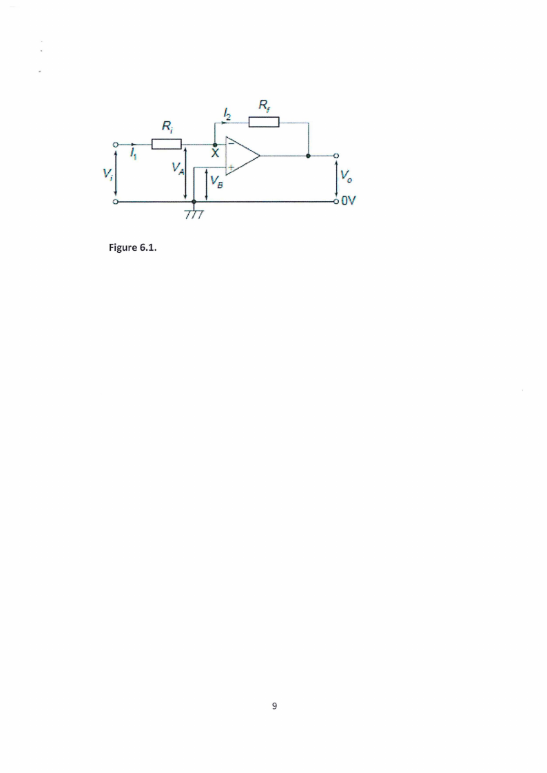
I
Figure 6.1.
9