


 |
COA511S - COMPUTER ORGANISATION AND ARCHITECTURE - 2ND OPP - DEC 2025 |
|
|
1 Page 1 |
▲back to top |
nAm l BI A UnlVERSITY
OF SCI EnC E Ano TECHnOLOGY
FACULTY OF COMPUTING AND INFORMATI CS
DEPARTMENT OF CYBER SECURITY
QUALIFICATION: BACHELOR OF COMPUTER SCIENCE, BACHELOR OF COMPUTER IN CYBER
SECURITY & BACHELOR OF INFORMATICS
QUALIFICATION CODE: 07BACS, 07BCCS &
07BAIF
LEVEL: 5
COURSE : COMPUTER ORGANISATION
AND ARCH ITECTURE
COURSECODE: COAS11S
DATE: December 2025
PAPER: THEORY
DURATION: 120 Minutes
MARKS: 100
SECOND OPPORTUNITY/SUPPLEMENTARY EXAMINATION QUESTION PAPER
EXAMINER(S) MR. JULIUS SILAA
MR. MBAUNGURAIJE TJUKUZU
MR. PETRUS KATAMBO
MR. IMMANUEL NAMPALA
MR JACKSON NGHIDULIKA
MS. SEPISO CHIKURUWO
MR. ANDREAS AMUKWA
MODERATOR: DR. SEBASTIAN MUKUMBIRA
THIS QUESTION PAPER CONSISTS OF 4 PAGES
(Excluding this front page)
INSTRUCTIONS
1. Answer ALL the questions on the answer scripts.
2. Write clearly and neatly.
3. Number the answers clearly.
PERMISSIBLE MATERIALS
1. None.
|
|
2 Page 2 |
▲back to top |
SECTION A [15 MARKS]: Answer All Questions. Each Question Weighs 1 Mark.
Indicate whether each of the following statements is True or False.
1. Unlike EEPROM, standard CD and DVD optical discs cannot be electrically erased and
rewritten. True/ False
2. Multiplexers are used in digital circuits to manage signal and data routing. True/ False
3. Read-only memory (ROM) is implemented using combinational circuits. True/ False
4. The address of the next instruction to be fetched is stored in the program counter.
True/ Fals.e
5. The use of addressing bits is determined solely by the number of operands. True/ False
6. Registers temporarily store data and instructions waiting to be processed by the ALU.
True/ False
7. A data register can only store data and cannot be used to calculate an operand's address.
True/ False
8. The hexa decimal equivalent of the binary number 10100101 is AS. True/ False
9. In floating-point arithmetic, a positive exponent surpassing the maximum allowed exponent
is called exponent overflow. True/ False
10. Super-pipelined architecture utilizes numerous, finely detailed pipeline stages. True/ False
11. The decode instruction phase determines both the opcode and the operand specifiers.
True/ False
12. Amdahl 's Law stat es that the speedup of a progra m using multiple processors in parallel
• computing is not limited by the fraction of the program that cannot be parallelized.
True/ False
13. The Arithmetic Logic Unit (ALU) performs the computer's data processing functions.
True/ False
14. A flip-flop exists in one of two states and remains in that state without (nput. True/ False
15. A thread is a dispatchable unit of work w ithin a process that has it s own processor context
and stack data area. True / False
SECTION B [15 MARKS]: Answer All Questions. Each Question Weighs 1 Mark.
Choose the correct answer for each of the following:
1. Component of t he CPU is responsible for performing arithmetic and logical operations?
A. Control Unit
B. Cache Memory
C. Arithmetic Logic Unit (ALU)
D. Instru ction Decoder
2.
Which factor influences t he number of bits used for addressing in a processor?
A. Instruction length
B. Memory size
C. Number of registers
D. All of th e above
3.
During instruction execution, which step involves retrieving the instruction from memory?
A. Fet ch instruction
Page 1 of4
|
|
3 Page 3 |
▲back to top |
B. Decode instruction
C. Execute instruction
D. Store result
4.
Which register holds the data temporarily before it is written to memory?
A. Program Counter
B. Instruction Register
C. Memory Buffer Register
D. Stack Pointer
5.
On an optical CD, what are t he tiny indentations that store data called?
A. Tracks
B. Pits
C. Grooves
D. Blocks
6.
Which CPU component acts as a high-speed storage area for frequently used data?
A. Cache Memory
B. Control Unit
C. System Bus
D.ALU
7.
What is the binary equivalent of the hexadecimal number 7B?
A. 01111011
B.10111011
C. 01110111
D.10011010
8.
Which register stores the address of the instruction to be executed next?
A. Memory Data Register
B. Instruction Register
C. Program Counter
D. Accumulator
9.
Which type of register is used to store the status of the CPU after an operation?
A. General Purpose
B. Data
C. Condition Code
D. Address
10. Which archit ecture allows multiple instructions to be executed simultaneously?
A. Superscalar
B. Single-cycle
C. Sequential
D. Multi-core
11. Which digita l ci rcuit component is used to select one of many input signals to pass to the
outp ut?
A. Decoder
B. Multiplexer
C. Register
D. Counter
Page 2 of4
|
|
4 Page 4 |
▲back to top |
12. In floating-point arithmetic, what occurs when the exponent is too small to be represented?
A. Exponent Overflow
B. Exponent Underflow
C. Significand Overflow
D. Significand Underflow
13. Which type of memory is non-volatile and cannot be modified during normal operation?
A. Random Access Memory
B. Cache Memory
C. Read Only Memory
D. Flash Memory
14. Which digital circuit component toggles its output based on a clock signal?
A. Latch
B. Flip-Flop
C. Multiplexer
D. Gate
15. The instruction register holds _ __ _
A. the address of the next instruction
B. the data to be processed
C. the current instruction being executed
D. the output of the ALU
SECTION C [70 MARKS] : Comprehension questions.
Question 1
[12 marks)
a) Discuss the concepts of paging and swapping in memory management, highlighting
their advantages and disadvantages.
(6 marks)
b) Briefly explain the three primary cache mapping schemes used to manage data
transfer between main memory and CPU cache.
(6 marks)
Question 2
[G marks]
The CPU is a critical component in any computer system, and efficient CPU utilization is crucial for
optimal performance. Compare and contrast Interrupt Driven with DMA 1/0 strategies focusing on
how each method impacts CPU usage.
(6 marks)
Question 3
[10 marks}
A delivery drone has 2 GB of memory. Suppose this memory is word addressable meaning that
every word has its own unique address for accessing it.
a) If each word in memory has its own address, how many total words can be stored in its
memory? (assume a standard word size of 4 bytes).
(4 marks)
b) Imagine this memory is organized into blocks, where each block holds 64 words. How
Page 3 of4
|
|
5 Page 5 |
▲back to top |
many blocks would this memory have?
(3 marks)
c) How many lines of cache memory will be req uired to accommodate all blocks
main memory in (b} above by using the direct cache addressing scheme? (3 marks)
Question 4
[6 marks]
a) Explain your understanding of Boolean algebra and Boolean identities, and describe how and
why they are used to model digital circuits. Provide examples and, where appropriate,
illustrations to support your explanation.
(6 marks)
Question 5
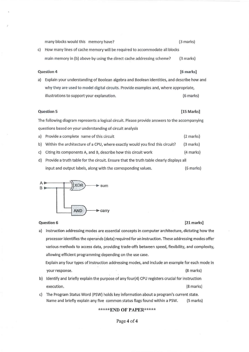
[15 Marks]
The following diagram represents a logical circuit. Please provide answers to the accompanying
questions based on your understanding of circuit analysis
a) Provide a complete name of this ci rcuit
(2 marks)
b) Within the architecture of a CPU, where exact ly would you find this circuit? (3 marks)
c) Citing its components A, and B, describe how this circuit work
(4 marks)
d) Provide a truth table for the circuit. Ensure that the truth table clearly displays all
input and output labels, along with the corresponding values.
(6 marks)
:-------B---sum
~ - - ~ND, •,____,_ carry
Question 6
[21 marks]
a) Instruction addressing modes are essential concepts in comput er architecture, dictating how the
processor identifies the operands (data) required for an instruction. These addressing modes offer
various methods to access data, providing t rade-offs between speed, flexibility, and complexity,
allowing efficient programming depending on the use case.
Explain any four types of instruction addressing modes, and include an example for each mode in
your response.
(8 marks)
b) Identify and briefly explain the purpose of any four(4} CPU registers crucial for instruction
execution.
(8 marks)
c) The Program Status Word (PSW) holds key information about a program's current state.
Name and briefly explain any five common status flags found w ithin a PSW. (5 marks)
*****END OF PAPER*****
Page 4 of4